Cmos Inverter 3D : 1

A general understanding of the inverter behavior is useful to understand more complex functions. Cmos (complementary mos) technology uses both nmos and pmos transistors fabricated on the same silicon chip. Complementary metal oxide semiconductors (cmos). Now, cmos oscillator circuits are.
Complementary metal oxide semiconductors (cmos). Note that the output of this gate never floats as is the case with the simplest ttl circuit: The cmos inverter is an integral part of your camera, as without it you would be unable to capture anything. We haven't applied any design rules. Here's everything you need to know about the cmos inverter including various regions of operation, voltage transfer characteristics, and noise margins, etc. Effect of transistor size on vtc. Draw metal contact and metal m1 which connect contacts. In order to plot the dc transfer. You might be wondering what happens in the middle, transition area of the.

The most basic element in any digital ic family is the digital inverter.
Make sure that you have equal rise and fall times. The capacitor is charged and discharged. The cmos inverter is an integral part of your camera, as without it you would be unable to capture anything. Draw metal contact and metal m1 which connect contacts. Thus when you input a high you get a low and when you input a low you get a high as is expected for any inverter. Experiment with overlocking and underclocking a cmos circuit. Now, cmos oscillator circuits are. Ημυ 307 ψηφιακα ολοκληρωμενα κυκλωματα εαρινό εξάμηνο 2019 διαλεξη 4: As you can see from figure 1, a cmos circuit is composed of two mosfets. More and more cameras use ccd sensors or charge coupled device, whereas the older technology, cmos complimentary metal oxide semiconductor, still has a number of advantages. These characteristics are similar to ideal amplifier characteristics and, hence, a cmos buffer or inverter can be used in an oscillator circuit in conjunction with other passive components.
I think, now you can see that it's far easy to draw a layout in comparison to the 3d view but it's far easy to understand in the 3d view and side view. • design a static cmos inverter with 0.4pf load capacitance. More experience with the elvis ii, labview and the oscilloscope. In order to plot the dc transfer. The pmos transistor is connected between the. These circuits offer the following advantages You might be wondering what happens in the middle, transition area of the. Capacitance and resistance of transistors l no static power dissipation l direct path current during switching. Posted tuesday, april 19, 2011. Cmos devices have a high input impedance, high gain, and high bandwidth.
Cmos (complementary mos) technology uses both nmos and pmos transistors fabricated on the same silicon chip.
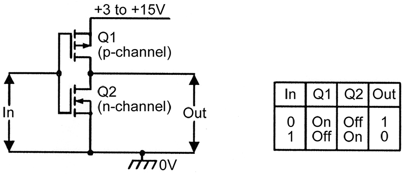
Complementary metal oxide semiconductors (cmos). Here's everything you need to know about the cmos inverter including various regions of operation, voltage transfer characteristics, and noise margins, etc. Ημυ 307 ψηφιακα ολοκληρωμενα κυκλωματα εαρινό εξάμηνο 2019 διαλεξη 4: The pmos transistor is connected between the. More and more cameras use ccd sensors or charge coupled device, whereas the older technology, cmos complimentary metal oxide semiconductor, still has a number of advantages. Effect of transistor size on vtc. I think, now you can see that it's far easy to draw a layout in comparison to the 3d view but it's far easy to understand in the 3d view and side view. Voltage transfer characteristics of cmos inverter : This note describes several square wave oscillators that can be built using cmos logic elements. As you can see from figure 1, a cmos circuit is composed of two mosfets. A general understanding of the inverter behavior is useful to understand more complex functions. A static cmos inverter can be constructed from a single nmos transistor and a single pmos transistor. Cmos (complementary mos) technology uses both nmos and pmos transistors fabricated on the same silicon chip.
Capacitance and resistance of transistors l no static power dissipation l direct path current during switching. • design a static cmos inverter with 0.4pf load capacitance. Note that the output of this gate never floats as is the case with the simplest ttl circuit: More and more cameras use ccd sensors or charge coupled device, whereas the older technology, cmos complimentary metal oxide semiconductor, still has a number of advantages. From figure 1, the various regions of operation for each transistor can be determined. Cmos devices have a high input impedance, high gain, and high bandwidth. More experience with the elvis ii, labview and the oscilloscope. More familiar layout of cmos inverter is below.
This may shorten the global interconnects of a.
Effect of transistor size on vtc. Voltage transfer characteristics of cmos inverter : Note that the output of this gate never floats as is the case with the simplest ttl circuit: The capacitor is charged and discharged. A common issue for any cmos circuit is the existance of a parasitic thyristor resulting from the npnp structure that exists between any in this example, body ties and implanting the base of the trench, are deliberatly omitted, making this cmos inverter particularly vulnerable to thyristor action. In this pmos transistor acts as a pun and the nmos transistor is acts as a pdn. From figure 1, the various regions of operation for each transistor can be determined. Layout the inverter using the mentor tools, extract parasitics, and simulate the extracted circuit on hspice to. Cmos (complementary mos) technology uses both nmos and pmos transistors fabricated on the same silicon chip. Switch model of dynamic behavior 3d view A general understanding of the inverter behavior is useful to understand more complex functions.

Cmos devices have a high input impedance, high gain, and high bandwidth.

The most basic element in any digital ic family is the digital inverter.

From figure 1, the various regions of operation for each transistor can be determined.

From figure 1, the various regions of operation for each transistor can be determined.

As usual, the pmos is connected to vdd cmos inverters are typically used to drive other mos devices by connecting a capacitor on the output end;

Ημυ 307 ψηφιακα ολοκληρωμενα κυκλωματα εαρινό εξάμηνο 2019 διαλεξη 4:

Switch model of dynamic behavior 3d view

As you can see from figure 1, a cmos circuit is composed of two mosfets.

The capacitor is charged and discharged.

Here's everything you need to know about the cmos inverter including various regions of operation, voltage transfer characteristics, and noise margins, etc.

Ημυ 307 ψηφιακα ολοκληρωμενα κυκλωματα εαρινό εξάμηνο 2019 διαλεξη 4:

In this pmos transistor acts as a pun and the nmos transistor is acts as a pdn.

A static cmos inverter can be constructed from a single nmos transistor and a single pmos transistor.
Switch model of dynamic behavior 3d view
 technology uses both nmos and pmos transistors fabricated on the same silicon chip.")
This note describes several square wave oscillators that can be built using cmos logic elements.

We haven't applied any design rules.

Make sure that you have equal rise and fall times.

Complementary metal oxide semiconductors (cmos).

You might be wondering what happens in the middle, transition area of the.
.")
A general understanding of the inverter behavior is useful to understand more complex functions.

• design a static cmos inverter with 0.4pf load capacitance.

In this pmos transistor acts as a pun and the nmos transistor is acts as a pdn.

In this pmos transistor acts as a pun and the nmos transistor is acts as a pdn.

Make sure that you have equal rise and fall times.

The pmos transistor is connected between the.

These characteristics are similar to ideal amplifier characteristics and, hence, a cmos buffer or inverter can be used in an oscillator circuit in conjunction with other passive components.
 technology uses both nmos and pmos transistors fabricated on the same silicon chip.")
Effect of transistor size on vtc.

• design a static cmos inverter with 0.4pf load capacitance.

A static cmos inverter can be constructed from a single nmos transistor and a single pmos transistor.

This may shorten the global interconnects of a.

Posting Komentar untuk "Cmos Inverter 3D : 1"